- 您现在的位置:买卖IC网 > Sheet目录1214 > EVAL-ADE7754EBZ (Analog Devices Inc)BOARD EVALAUTION FOR ADE7754
�� �
�
�ADE7754�
�t� 8�
�CS�
�SCLK�
�t� 1�
�t� 2� t� 3�
�t� 4�
�t� 5�
�t� 7�
�t� 7�
�t� 6�
�DIN�
�1�
�0�
�A5�
�A4�
�A3�
�A2�
�A1�
�A0�
�DB7�
�DB0�
�DB7�
�DB0�
�COMMAND� BYTE�
�MOST� SIGNIFICANT� BYTE�
�LEAST� SIGNIFICANT� BYTE�
�Figure� 44.� Serial� Interface� Write� Timing� Diagram�
�SCLK�
�DIN�
�X�
�X�
�X�
�X�
�DB11� DB10�
�DB9�
�DB8�
�DB7�
�DB6�
�DB5�
�DB4�
�DB3�
�DB2�
�DB1�
�DB0�
�MOST� SIGNIFICANT� BYTE�
�LEAST� SIGNIFICANT� BYTE�
�Figure� 45.� 12-Bit� Serial� Write� Operation�
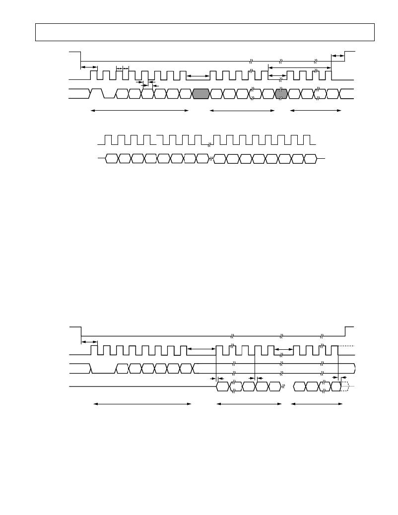
�Serial� Read� Operation�
�During� a� data� read� operation� from� the� ADE7754,� data� is� shifted�
�out� at� the� DOUT� logic� output� on� the� rising� edge� of� SCLK.� As�
�was� the� case� with� the� data� write� operation,� a� data� read� must� be�
�preceded� by� a� write� to� the� communications� register.�
�With� the� ADE7754� in� communications� mode� and� CS� logic� low,�
�an� 8-bit� write� to� the� communications� register� first� takes� place.�
�The� MSB� of� this� byte� transfer� must� be� a� 0,� indicating� that� the�
�next� data� transfer� operation� is� a� read.� The� six� LSBs� of� this� byte�
�contain� the� address� of� the� register� to� be� read.� The� ADE7754�
�starts� shifting� out� of� the� register� data� on� the� next� rising� edge� of�
�SCLK.� See� Figure� 46.� At� this� point,� the� DOUT� logic� output�
�switches� from� high� impedance� state� and� starts� driving� the� data�
�bus.� All� remaining� bits� of� register� data� are� shifted� out� on� subsequent�
�SCLK� rising� edges.� The� serial� interface� enters� communications�
�CS�
�t� 1�
�SCLK�
�t� 9�
�mode� again� as� soon� as� the� read� has� been� completed.� The� DOUT�
�logic� output� enters� a� high� impedance� state� on� the� falling� edge� of�
�the� last� SCLK� pulse.� The� read� operation� may� be� aborted� by�
�bringing� the� CS� logic� input� high� before� the� data� transfer� is� com-�
�pleted.� The� DOUT� output� enters� a� high� impedance� state� on� the�
�rising� edge� of� CS� .�
�When� an� ADE7754� register� is� addressed� for� a� read� operation,�
�the� entire� contents� of� that� register� are� transferred� to� the� serial�
�port.� This� allows� the� ADE7754� to� modify� its� on-chip� registers�
�without� the� risk� of� corrupting� data� during� a� multibyte� transfer.�
�Note� that� when� a� read� operation� follows� a� write� operation,� the�
�read� command� (i.e.,� write� to� communications� register)� should�
�not� happen� for� at� least� 1� μ� s� after� the� end� of� the� write� operation.�
�If� the� read� command� is� sent� within� 1� μ� s� of� the� write� operation,�
�the� last� byte� of� the� write� operation� may� be� lost.�
�t� 10�
�DIN�
�0�
�0�
�A5�
�A4�
�A3�
�A2�
�A1�
�A0�
�t� 11�
�t� 12�
�t� 13�
�DOUT�
�DB7�
�DB0�
�DB7�
�DB0�
�COMMAND� BYTE�
�MOST� SIGNIFICANT� BYTE�
�LEAST� SIGNIFICANT� BYTE�
�Figure� 46.� Serial� Interface� Read� Timing� Diagram�
�REV.� 0�
�–29� –�
�发布紧急采购,3分钟左右您将得到回复。
相关PDF资料
EVAL-ADE7755ZEB
BOARD EVALUATION FOR AD7755
EVAL-ADE7758ZEB
BOARD EVAL FOR AD7758
EVAL-ADE7759EBZ
BOARD EVALUATION FOR ADE7759
EVAL-ADE7762EBZ
BOARD EVALUATION FOR ADE7762
EVAL-ADE7763ZEB
BOARD EVALUATION FOR ADE7763
EVAL-ADE7816EBZ
BOARD EVALUATION FOR ADE7816
EVAL-ADE7878EBZ
BOARD EVAL FOR ADE7878
EVAL-ADE7880EBZ
BOARD EVAL FOR ADE7880
相关代理商/技术参数
EVAL-ADE7755EB
制造商:Analog Devices 功能描述:EVAL BOARD ENERGY METERINGW/PULSE OUTPUT - Bulk
EVAL-ADE7755EBZ
制造商:AD 制造商全称:Analog Devices 功能描述:Energy Metering IC with Pulse Output
EVAL-ADE7755EBZ1
制造商:AD 制造商全称:Analog Devices 功能描述:Energy Metering IC with Pulse Output
EVAL-ADE7755ZEB
功能描述:BOARD EVALUATION FOR AD7755 RoHS:是 类别:编程器,开发系统 >> 评估演示板和套件 系列:- 标准包装:1 系列:- 主要目的:电信,线路接口单元(LIU) 嵌入式:- 已用 IC / 零件:IDT82V2081 主要属性:T1/J1/E1 LIU 次要属性:- 已供物品:板,电源,线缆,CD 其它名称:82EBV2081
EVAL-ADE7756EB
制造商:Analog Devices 功能描述:EVAL BD DOCUMENTATION ADE7756 ENERGY METERING IC - Bulk 制造商:Rochester Electronics LLC 功能描述:
EVAL-ADE7757AEBZ
制造商:Analog Devices 功能描述:EVALUATION BOARDS - Bulk
EVAL-ADE7757EB
制造商:Analog Devices 功能描述:EVAL BOARD ENERGY METERINGW/PULSE OUTPUT - Bulk
EVAL-ADE7758ZEB
功能描述:BOARD EVAL FOR AD7758 RoHS:是 类别:编程器,开发系统 >> 评估演示板和套件 系列:* 标准包装:1 系列:PSoC® 主要目的:电源管理,热管理 嵌入式:- 已用 IC / 零件:- 主要属性:- 次要属性:- 已供物品:板,CD,电源